Spatially-resolved band gap and dielectric function in 2D materials from Electron Energy Loss Spectroscopy
This is a summary highlighting the application of EELSFitter in this publication. For more detail about the work presented, please refer to the publication itself [Brokkelkamp et al., 2022]
Abstract
The electronic properties of two-dimensional (2D) materials depend sensitively on the underlying atomic arrangement down to the monolayer level. Here we present a novel strategy for the determination of the band gap and complex dielectric function in 2D materials achieving a spatial resolution down to a few nanometers. This approach is based on machine learning techniques developed in particle physics and makes possible the automated processing and interpretation of spectral images from electron energy loss spectroscopy (EELS). Individual spectra are classified as a function of the thickness with K-means clustering, and then used to train a deep-learning model of the zero-loss peak background. As a proof of concept we assess the band gap and dielectric function of InSe flakes and polytypic WS2 nanoflowers and correlate these electrical properties with the local thickness. Our flexible approach is generalizable to other nanostructured materials and to higher-dimensional spectroscopies and is made available as a new release of the open-source EELSfitter framework.
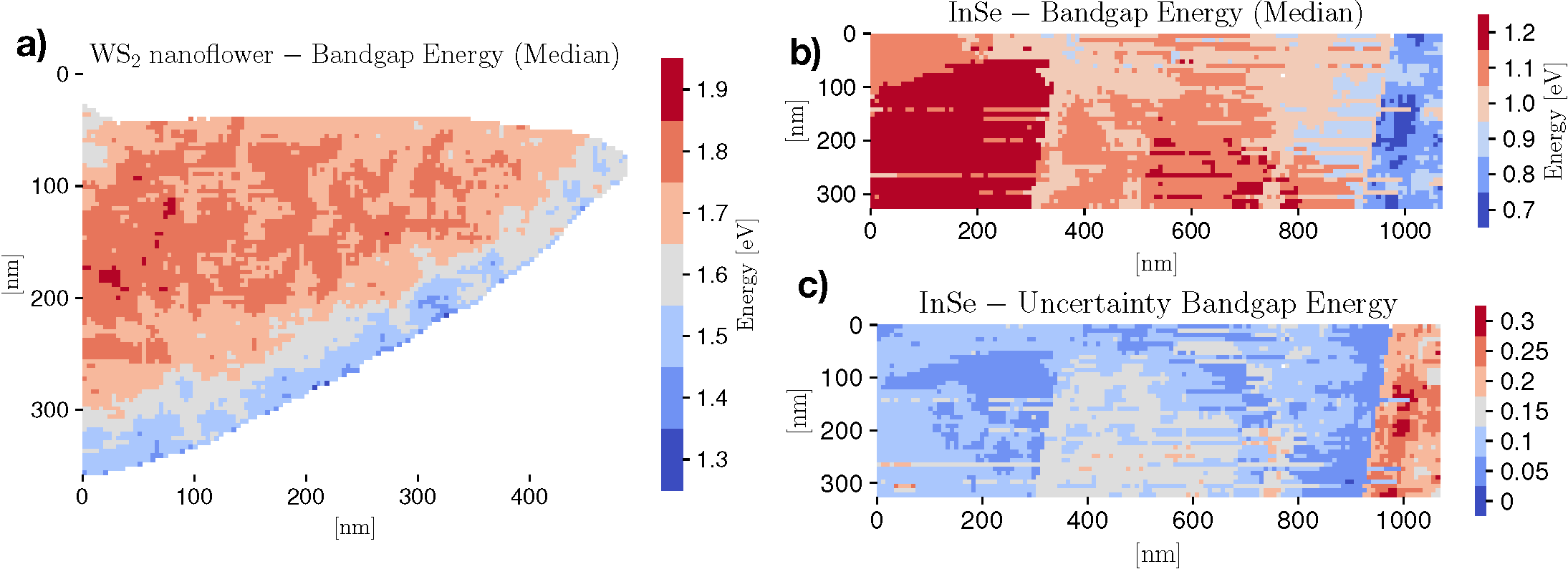
Fig. 9 (a) Spatially-resolved map of the bandgap for the WS2 nanoflower specimen, where a mask has been applied to remove the vacuum and pure substrate pixels. (b,c) The median value of the bandgap energy \(E_{bg}\) and its corresponding 68% CL relative uncertainties across the InSe specimen, respectively.